PCB edge plating is the process of plating exposed copper connections along the edges of a printed circuit board with a metallic coating like gold or tin to facilitate electrical connections. This article provides a comprehensive overview of PCB edge plating including its purpose, edge connector types, plating processes, inspection, reliability factors, and future trends.
A PCB edge connector refers to the gold plated contact fingers or pads arrayed along one or more edges of a circuit board that mate with a corresponding connector. The board edge fits into a slot to make electrical contact.
Edge connectors allow boards to be easily installed, removed, and replaced from electronic systems.
Key benefits of edge connectors:
Allow insertion/removal of PCBs from system
Wipe contact action for reliable connections
Component-less connections simplify assembly
Easy to fabricate and integrate on PCB
No soldering required
Withstand thousands of mating cycles
Support high density contact configurations
Enable high frequency signaling
These factors make edge connectors highly versatile and cost-effective.

Common edge connector configurations include:
One row of contacts on board edge
Less costly, lower density
Used for prototypes or low complexity
Two parallel rows of staggered contacts
Allows higher number of connections
Improves mechanical alignment
More than two rows, or rows on multiple edges
Further increases connection density
Complex PCB layout
Very narrow pitch between contacts
Up to 600+ connections on single edge
May use dual-beam cantilever contacts
To provide conductivity and protect copper traces, edge contacts require metallic plating like:
Gold – Most common, resistant to oxidation/corrosion
Tin – Lower cost but susceptible to oxidation over time
Palladium-Nickel – Avoid tin whisker issues, lower cost
Gold Flash over Nickel – Combines low cost nickel with gold outer layer
A minimum thickness like 50 μin of gold ensures durability over 10,000+ mating cycles.
A typical PCB edge plating process involves:
Drilling holes for edge contacts
Copper electroless then electrolytic plating
Etching to form isolated traces
Surface preparation like microetching
Immersion plating of gold or other metal
Cleaning then drying boards
Quality inspection – thickness, continuity, defects
Electrical testing if needed
Fabrication generally follows standard PCB methods plus final plating.
Key process controls needed:
Plating Thickness – Confirm minimum thickness met via microscopy or X-ray fluorescence. Insufficient plating risks wear or corrosion issues.
Continuity – Verify electrical connectivity from inner layers through plated edge contacts.
Plating Coverage – Inspect for voids or thin areas around traces.
Overplating – Ensure plating does not excessively build up on glass weave. Can impede mating.
Trace Geometry – Confirm dimensions match specifications.
Several factors impact connector lifespan:
Plating thickness – Thicker gold or tin plating improves cycle life and durability.
PCB thickness – Boards thinner than 1 mm may bow during mating stress.
Contact geometry – Well-designed trace shapes tolerate repeated mating forces.
Receptacle contacts – Select robust and proven connector contact designs to match.
Contamination – Prevent dirt, oils, or particles during handling and use.
Key checks on completed connectors:
Continuity – Spot check electrical conductivity through mated connection.
Contact Engagement – Confirm full insertion with visual checks.
Marks/Damage – Inspect for signs of wear, scrapes, or damage after assembly cycles.
Contamination – Verify absence of particles or films from handling.
Key specifications and standards for edge connectors:
IPC-2223 – Sectional requirements for PCB edge contacts
IPC-6013 – Qualification and performance of edge connections
IPC/EIA J-STD-002 – Solderability tests for component leads/terminations
IEC 60352-5 – Reliability testing and requirements
Compliance to standards ensures quality and reliability goals are met

To optimize edge connector performance:
Minimize total board thickness
Ensure adequate board rigidity
Include integrated stiffener ribs if needed
Avoid placing components along connector edge
Include generous fillets at trace corners
Fanout inner layer traces gradually
Reviewing layouts with the receptacle supplier is recommended.
Edge connectors see wide usage across:
Computers – Daughtercards, memory modules, backplanes
Telecom – Switching cards, router cards, base stations
Military/Aerospace – Mission systems, navigation cards
Medical – MRI, ultrasound, imaging cards
Automotive – Engine control units, instrument clusters
Consumer – Set-top boxes, game consoles
Edge connectors enable quick field replacement of electronics cards or modules across industries.
Edge connector technology continues advancing:
Increasing Density – More contacts in thinner boards enabling complex interconnection.
Higher Frequencies – Extending signal integrity to 10+ Gbps rates.
Improved Durability – Advanced plating and contact shaping for 10,000+ mating cycles.
Lower Costs – Simplified fabrication allowing broader adoption.
Connector manufacturers and PCB fabricators are driving progress.
In summary, PCB edge plating and connectors offer a versatile and cost-effective interconnection method widely used for replaceable subsystems, cards, and modules across many industries. Edge connectors will continue meeting the challenges of denser contacts, thinner boards, faster signaling, and improved reliability thanks to ongoing advancements in plating technology, board materials, and precision manufacturing techniques. While alternative approaches like board-to-board connectors exist, the simplicity and convenience of edge connectors ensures their usage well into the future anytime field replaceability of circuits is required.
Q: What is the most common metal used for edge connector plating?
A: Gold is by far the most popular thanks to its durability and resistance to corrosion and oxidation over thousands of mating cycles.
Q: What are some key reliability concerns with edge connectors?
A: Insufficient plating thickness, contamination, poor contact design, and inadequate board thickness or rigidity impact connector lifespan.
Q: How many mating cycles can a robust edge connector withstand?
A: Well designed gold plated connectors using suitable PCB thickness can achieve 10,000 cycles or more.
Q: What are some alternatives to PCB edge connectors?
A: Board-to-board connectors, hybrid edge connectors, and high density board stacking connectors offer other options.
Q: What is the main benefit of using dual row edge connectors versus single row?
A: Dual row configurations double the connection density by interleaving two staggered rows of contacts.
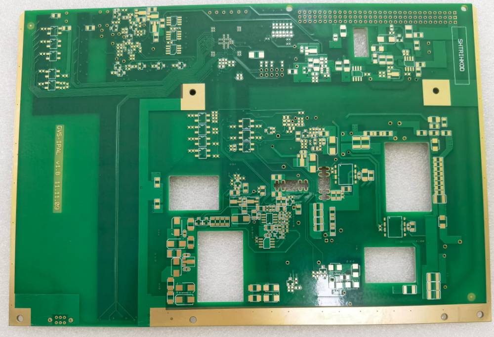
At present, there are two kinds of PCB board edge design: metallization and non-metallization. For non-metallization, manufacturers in the industry have matured, but the metallization technology is still immature. Nowadays, more customers’ production needs are turning to PCB metal edging. Therefore, the quality of PCB metal edging has become the focus of customers’ and manufacturers’ attention because its quality directly affects the use of products.
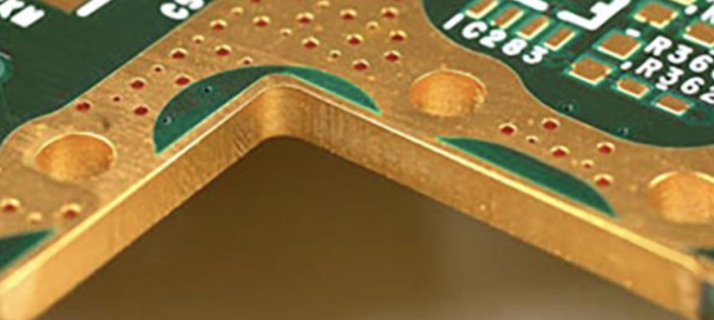
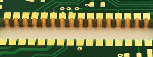
Metalized edging means that the edge of the board must be metalized. English description: Edge plating, border plated, plated contour, side plating, side metal, etc.
More electronic products start to minimize the product volume as the goal so that PCB will use electroplated nickel and gold surface treatment(ENIG) technology. In the production process, the gold-plated finger process can achieve the gold-cladding of the solder joints. Still, it is necessary to separately make the lead-through solder joints and the board edges, even though they are removed after gold plating. It is only convenient for the production of gold-clad solder joints on the side of the board. The production process of electroplating nickel gold is simple. It is unnecessary to make the leads separately, but only the top layer of the solder joints can be plated with gold, and the side plated with gold can not be produced. The gold-plated nickel-gold plating process on the side of the circuit board can achieve the top layer gold plating and the side-side gold plating at the same time.
Drilling —- Milling metalized slot hole —- Removing dirt —- Plated-through hole
Determine the area where the board needs to be metalized.
When most customers are designing the circuit, the copper is stretched out on the outer edge of the board. When this happens, you need to consider whether the edge of the board needs to be hemmed and if the metalized edging is needed during production (must require formal instructions from the customer).
Sources of information: One is Gerber files, and the others are PDF, TXT, DWG, etc.
Design and precautions of metallized edging board
Copy the outline layer in the design file to the pthrou layer to make a closed long slot.
Note that since copper plating is required at the encapsulation, the copper thickness has a specific thickness. Therefore, when making the hemming shape, compensation should be considered.
After finishing the edging groove, the next step is to determine the electrical connectivity of the edging.
In order to determine which layer should be connected to the hemming, the following sequence should be followed:
Find out which layers and areas the customer requires to connect.
Clear the connection requirements of each layer.
Precautions for the production of metalized edging lines
For the edged board, in order to prevent film chipping, it is necessary to ensure that the pad is 10MIL on one side. Whether in the board, on the side, or outside the board, it must have a 10MIL pad. If it needs to be added or changed, it must be confirmed by the customer. If there are pads near the edging, the pads’ distance and the edging disk should be at least 8MIL. If it cannot be satisfied, feedback and confirmation are required.
After the hemming, the connection of the inner and outer layers must be checked. The connection method between the layers must be determined to avoid electrical and ground short circuits after the hemming.
If there is a plated film, the edging must be processed like a PTH groove, and there must be a disk. Pay special attention: the edging of the special-shaped groove should also be the same as the hole, which needs to be filled and enlarged by 4mil.
Solder mask design for metallized edging
For the solder mask, the edging groove must be fully windowed.
Bounding solder mask opening = Bounding pad +0.16mm

In order to improve production efficiency, CAM must use standard milling cutters to make edging grooves, such as: 0.8, 1.0, 1.6, 2.0, 2.4mm.
Remarks: If this is not in the customer’s requirement, please choose 2.0mm or greater.
The long direction of the edging slot must be parallel to the long side of the rear panel (the direction of the edging slot is parallel to the running direction of the tin spray).
For orders that do not meet the above requirements, the project pre-review will require the customer to confirm the use of non-sprayed surface processes such as gold or copper-nickel plating.
Other matters needing attention
If the antenna position is too large, it will affect the customer’s welding or signal transmission.
The inner cladding pad is connected to the wire in the board, causing a Short circuit.
The stamp hole is designed at the edging slot, which must be treated with two drills.
Remarks:
If the stamp hole is placed in a drill, the plate may break due to the irregular forces when the plate swings back and forth in the electroplating cylinder.
If the bridge width is insufficient when spraying tin, the plate may break due to the force of the wind knife when spraying tin.

The process of plating the sidewalls of the circuit board with gold and electroplating nickel and gold includes:
Etching – Forms an etching groove on the copper surface of the circuit board. The etching groove extends along the pattern to be coated with gold on the sidewall, so that the copper layer needs to be coated with gold.
The side walls are exposed – A dry film is pasted on the copper layer, and an opening is formed on the dry film. The opening corresponds to the etching groove and the area of the copper plate surrounded by gold that needs to be covered with gold.
Expose the side walls – Electroplating the circuit board so that the copper plate area and the side walls are plated with a layer of nickel and gold.
If the copper plate area is an independent pad, lead is separately added.
The distance between the circumferential edge of the window and the circumferential edge of the copper plate area is 4 mils.
During electroplating, nickel and gold are formed on the upper surface and sidewalls of the copper plate area at the same time to achieve the top layer gold plating and the sidewall gold coating.

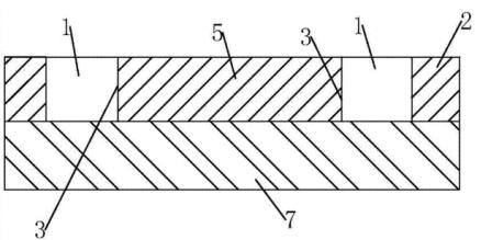
Reference signs in the figure: 1. Etching groove, 2. Copper layer, 3. Sidewall, 4. Dry film, 5. Copper plate area, 6. Open window, 7. Substrate, 8. Open window, 9. Dry film.
Specific operation instructions:
The gold plating nickel-gold electroplating process on the sidewall of the circuit board includes: Forming an etching groove (1) on the copper surface of the circuit board by etching. The etching groove (1) extends along the pattern to be coated with gold on the side of the board; this is why the copper layer (2) is required. The gold-clad sidewall (3) is exposed, and a dry film (4) is pasted on the copper layer (2). An opening (6) is formed on the dry film (4), which corresponds to the etching groove (1) and its surroundings. The copper plate area (5) that needs to be coated with gold is provided and exposed to the side walls. The circuit board is electroplated with nickel and gold so that both the copper plate area (5) and the side walls (3) are plated with a layer of nickel and gold.
When making a circuit board, as shown in Figure 1, paste a dry film (9) on the outer sidewall of the copper layer (2). Form an opening (8) on the dry film (9), which corresponds to the to-be-formed etching groove (1) and shape. Then, etching is performed, thereby forming an etching groove (1). One side wall (3) of the etching groove (1) needs to be side-clad with gold in the subsequent process.
Then, a dry film (4) is pasted on the outer wall of the copper layer (2). Simultaneously, the dry film (4) is formed with a window corresponding to the copper plate area (5) to be gold-plated, gold-clad on the side of the board, and the etching groove (1) around it.
Finally, it’s time to electroplate the circuit board. Since the upper surface and side surfaces of the copper plate area (5) are not covered with the dry film (4), nickel and gold can be formed on the upper surface and sidewalls of the copper plate area (5) during electroplating. This is to achieve top-layer gold plating and board edge gold plating at the same time.
Preferably, if the copper plate area (5) is an independent pad, a lead is added separately.
Preferably, the distance between the circumferential edge of the window (6) and the circumferential edge of the copper plate area (5) is 4 mils. In this way, it is convenient for the syrup to enter the pad’s sidewall position, and gold-cladding on the side of the board is achieved when electroplating is complete.
A process for coating the sidewalls of a circuit board with gold and electroplating nickel and gold is characterized in that it comprises:
An etching groove is formed on the copper surface of the circuit board by etching. The etching groove extends along the pattern to be coated with gold on the sidewall. This exposes the sidewall of the copper layer that needs to be coated with gold.
Paste a dry film on the copper layer, and form a window on the dry film. The window corresponds to the etching groove and the area of the copper plate that needs to be covered with gold and exposed to the sidewall.
Electroplating the circuit board with nickel and gold so that the copper plate area and the sidewall are plated with a layer of nickel and gold.
The process of plating the sidewall of the circuit board with gold and electroplating nickel and gold is that the distance between the circumferential edge of the window opening and the circumferential edge of the copper plate area is 4 mils.
With the increase of system speed, the timing and signal integrity problems of high-speed digital signals are important, but the EMC problems caused by the electromagnetic interference and power integrity in the system are also critical. The electromagnetic interference generated by the high-speed digital signal will cause serious mutual interference within the system and reduce the system’s anti-interference ability and generate strong electromagnetic radiation to the outer space.
This causes the system’s electromagnetic radiation emission to seriously exceed the EMC standard, making the product unable to pass EMC standard certification. The side-board radiation of a multilayer PCB is a relatively common source of electromagnetic radiation. When the unexpected current reaches the edge of the ground plane and the power plane, edge radiation occurs. The PCB board metalization edging process encloses the entire board edge with metal, so that the microwave signal cannot be radiated from the PCB board edge, thereby solving the problem of edge radiation. Of course, the use of the board edge metallization edging process will also increase the manufacturing cost of the PCB.
RayMing Electronics Co., Ltd. is a professional manufacturer of high-precision multilayer circuit boards, module immersion gold circuit boards, automotive circuit boards, driving recorders, COB power supplies, computer motherboards, medical circuit boards, module bonding boards, blind hole impedance board, thermoelectric separation copper substrate, etc. RayMing provides top-notch quality assurance and punctual delivery, a high-tech enterprise with sales as a whole. If there is a demand for side-coated gold boards, please feel free to contact us!
Contact: Michael
Phone: +8615338012748
E-mail: Michael@wydcircuits.com
Add: Address: B2-1, Building B2, WanXia Industrial Park, Tangwei, Fuyong Town, Baoan, Shenzhen, China.